


12-30-2015: Nano Dimension filed patent for 3D printing multimaterial electrical conductors
This method enabled the simultaneous printing of conductive and insulating materials

On December 30, 2015, Nano Dimension announced the submission of a patent application to the United States Patent and Trademark Office for a 3D printing technology capable of producing models with embedded electrical conductors. This innovative method enabled the simultaneous printing of conductive and insulating materials, paving the way for new possibilities in electronics design and manufacturing.
There was a time in the history of 3D printing when the Israeli company was developing and producing proprietary technological solutions, rather than frantically acquiring other companies in the AM market—sometimes successfully, sometimes not...
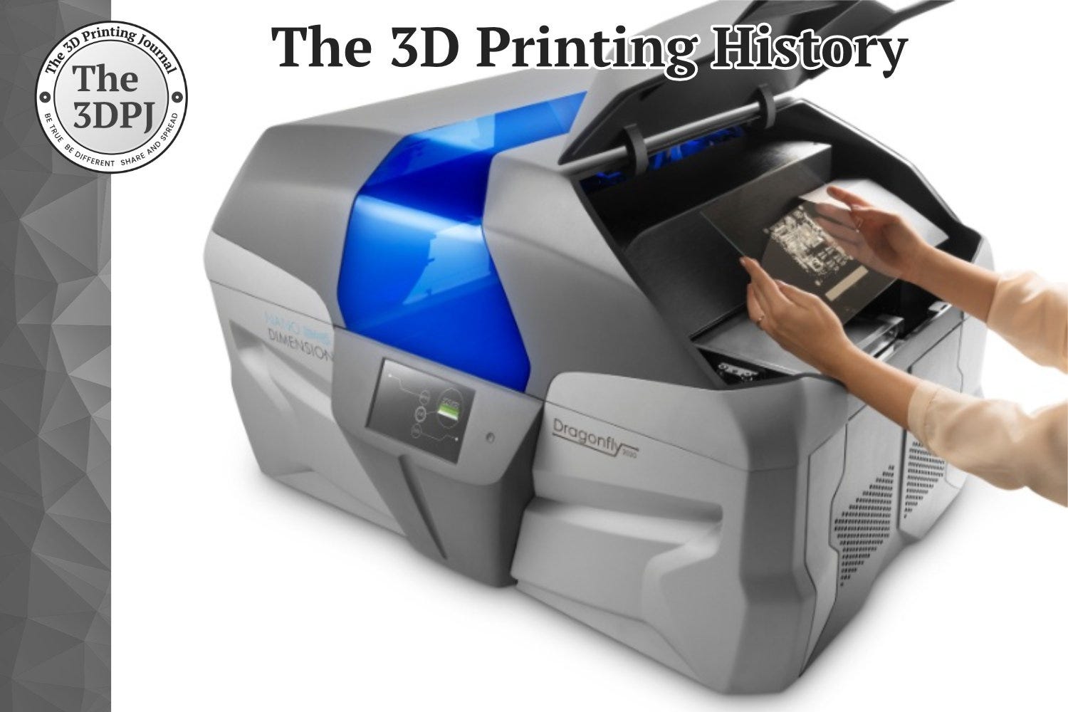
In those earlier days, the company, founded in Israel in 2012, was a leader in additive electronics manufacturing. Nano Dimension combined three advanced technologies: ink-based 3D printing, specialized software, and nanomaterials. Its flagship product was the first 3D printer dedicated to multilayer printed circuit boards (PCBs), along with nanoparticle-based conductive and dielectric inks.
The solution patented at the end of December 2015 had a key feature: the sintering of metallic conductors printed within a 3D polymer. This technology made it possible to create complex interconnections in a single production process and to embed conductors directly into the three-dimensional structures of objects.
This innovation allowed for the production of unconventional electronic products, unattainable through traditional manufacturing methods. The technology found applications in printing custom circuits and manufacturing structural objects with integrated electronics.
The development of this technology revolutionized several industries, including automotive, aerospace, and healthcare, by enabling the creation of more complex and compact electronic devices. During this period, Nano Dimension also utilized nanotechnology to produce oxidation-resistant inks and developed the DragonFly 2020 printer—the first device capable of printing multilayer PCBs in an office environment.
Source: www.nano-di.com